

"Did you know?" questions play a crucial role in bridging the knowledge gap for design engineers and buyers, enabling them to uncover valuable insights that can enhance decision-making. By staying updated on industry trends, technological advancements, and sustainability practices, they can foster innovative designs while making cost-effective purchasing choices, ensuring that both environmental considerations and competitive edge are maintained in their projects.

Did You Know?


-
What is Bare Die? Where is it used? What are the benefits of using Bare Die? These are questions that many design engineers and buyers ask. Unless you have been doing this for a good number of years you will quickly find out that there is a lot more involved than just searching for a Part# on the Internet. The trick is understanding the differences between packaged parts and bare die. Bare Die is used in a broad array of industries, and markets, including Aerospace, Military, Avionics, Medical Implant, Automotive, and high-end Industrial where bare die is the optimum choice for a given design.
SECTION 1:
Reasons To Use Bare Die
Smaller Size and Weight - Using bare die can allow for reduced board space.
Operating Temperature Size - Package thermal characteristics no longer inhibit the performance of the die or the environments where they can operate.
Ruggedness - Direct die attach and wirebond provides protections against high levels of shock and vibration.
Lighter Weight - Smaller designs and higher densities reduce weight and size of your application.
More Efficient Performance - Removing extra package interconnect can reduce capacitance and inductance.
Reliability - The reduced number of interconnects with die use leads to improved reliability. The typical packaged part has three connection points per I/O. Compare this with only two for wire bonds.
Electrical Performance - The lower inductance and capacitance of bare die is important in analog, RF, and power applications. Faster signal flight time (lower propagation delay) and improved power/ground distributions.
Hermetically Sealing - Air tight sealed packages can be selected that can be injected with inert gasses.
These die advantages promote higher levels of integration, improved electrical and reliability performance, and increased functionality per square area. The benefits of using unpackaged die in embedded designs can be substantial. The availability of IC products in die form gives customers a convenient option for small-footprint designs, enabling them to optimize their product designs for limited space and to implement innovative, proprietary packaging solutions.
SECTION 2:
The Secret of Specifying and Obtaining the Correct Bare Die to Build Hybrid Microcircuits
What is Bare Die? How do I buy Bare Die?
Unless you have been doing this for a good number of years you will quickly find out that there is a lot more involved than just searching for a Part# on the Internet. It’s especially frustrating to find out that in a world of “packaged” semiconductors that Bare Die commerce is perceived as a bother. The trick is understanding the differences between packaged parts and bare die.
Manufacturers produce a wafer that yields the die. After testing the wafer, individual die are separated from the wafer and assigned a part number and then shipped to a bare die distributor. Here, samples from a die lot are packaged to expedite Lot Acceptance Testing (LAT). Additional testing is usually done through a method of Known Good Die (KGD).
First, find a trusted Bare Die supplier that can provide you with the components in die form. Their expertise and advice will help you in the buying process. You may need Certificates of Conformance, Lot Traceability, Source Control Drawings, Geometries, Specific Testing performed. It can be very confusing.
Manufacturers produce a wafer that yields the die. After testing the wafer, individual die are separated from the wafer and assigned a part number and then shipped to a bare die distributor. Here, samples from a die lot are packaged to expedite Lot Acceptance Testing (LAT). Additional testing is usually done through a method of Known Good Die (KGD).
At the distributors facility, the die is visually reinspected to make sure that the die that you purchase looks flawless and will function well. In some instances, additional electrical testing is also performed for screening of specific electrical parameters. Current die geometries must be obtained and any changes that have occurred must be forwarded to the end customer for review and approval. Often times samples are required by the end customer. Depending on the device, the distributors can usually provide the required sample. Sometimes though, the part is not available from the manufacturer in die form, or if the manufacturer agrees to provide the part, the minimum purchase quantity may be much, much higher than the end customer requires. Always keep in mind that everything is NOT available in die form.
Specifying and obtaining the correct bare die to build hybrid microcircuits and multi-chip modules presents some specific problems. Dominant design factors here are hermetic sealing requirements, size, and weight. However, the special needs related to the supply of bare die continues to mystify much of the electronics community beyond the handful of hybrid manufacturers specifically focused on this market.
Most hybrids are designed around the characterization of packaged parts. Once samples are received, the function designer builds the breadboard, runs characterization data, and then asks the hybrid designers to create a hybrid or multi-chip module to simulate the function. Here is where the die distributor immediately begins to add value.
Taking the Bill Of Materials (BOM) from the customer, we immediately determine which of the requested parts are not readily available in die form or require added value processing. First, some semiconductor devices are not available as bare die because the manufacturer simply elects not to offer the device in die form. Many newer power discrete devices are assembled in packages that use a braised clip for the top contact attachment point. The top metal used to facilitate these packages is not suitable for wire bonding or soldering, so the manufacturer will not offer this die to the market.
In this era of large wafer diameters of 6-in. or 8-in. and larger, the manufacturer may elect not to 100 percent-probe smaller die at the wafer level. The manufacturer does sample probes only, and accepts the predicted yield loss during 100 percent test of the packaged part.
In some cases, parts that have no prior history in the die market may have prohibitively high minimum order requirements in die or wafer form from the manufacturer, making it impossible to sample or support prototype builds.
The die distributor can address each of these problems and either perform the required added value or recommend a list of alternatives that are more readily available. In the case where a manufacturer will simply not quote a bare die, the die distributor often has access to alternative sources that can offer die with similar functions.
Suitability for Wire Bonding
Where the top metal is not suitable for wire bonding, it is usually not difficult to find a similar device within the vendor portfolio that is offered in die form with the preferred metallization. In the case where 100 percent probe is not performed by the manufacturer, the die distributor can offer this service using in-house capabilities or outsourcing to an approved test lab. This also involves the distributor performing a Lot Acceptance Test (LAT) after probe, to provide objective evidence that the probe successfully met the specified requirements.
Stocking and Inventory Control
At ES Components, we have proactively identified a long list of popular devices throughout our line card and established an “off-the-shelf” inventory. This inventory is automatically replenished based on a predetermined min/max rather than market demand. An off-the-shelf part is immediately available for sampling and has virtually no Minimum Order Quantity (MOQ) when supporting prototype procurements. The products offered include a variety of analog microcircuits and a compete portfolio of popular discrete die and thin film resistor chips. We use this preferred inventory to quickly offer the hybrid designer alternatives that are readily available and provide a cost-effective solution. If the customer is unable to use one of these devices, we then support the procurement of a different required device.
Are you soldering to the top contact or wire bonding?
This is a must if there are any power discrete devices on the BOM. Many discrete die are available with either option. The rest are only offered with one or the other of these two options. If only solderable top metal is available, and there are no alternative devices, the die distributor can possibly offer a sub-assembly using a Copper or Molybdenum disk with suitable top plating to meet wire bond requirements.
How are you planning to attach the die?
The vast majority of power discretes are available from the manufacturer with solderable back metal only, some with either solderable or gold back metal. If the user is planning to use epoxy attach, it is highly recommended that they not use die with solderable metals. Gold back metal is recommended for either eutectic or epoxy attach. At ES Components we have developed and qualified the ability to remove solderable back metal from wafers and deposit gold for devices where this option is not available from the vendor. Silicon back die are generally epoxy-attached and if a eutectic attach is required, a gold alloy preform is needed.
How will you want this bare die packaged for delivery in full production?
Packaged parts are typically supplied in production quantities on tape-and-reel with nearly infinite shelf life. Waffle packs are the most common medium for shipping bare die, but high volume automatic assemblies are moving towards sawn wafer on film to reduce cost and enhance manufacturing throughput. However, sawn wafer on film has shelf life limitations which demand special management of the supply pipeline. A die distributor can manage the pipeline so that probed unsawn wafers are kept in stock in the appropriate environment and sawn wafers on film are limited to only those wafers needed for short-term production. If there is a delay in manufacturing, the unsawn wafer inventory remains pristine and the shelf life issue is confined to a small subset of the inventory.
Summary
By answering these questions at the time of initial contact and early in the design process, it’s possible to save the user time and money by avoiding the need to modify or redesign the function based on sample evaluation possibly weeks or even months later. We can also properly code the die part number to capture all the pertinent information for future reference.
ES Components is a trusted Bare Die supplier that will help you obtain the expertise and advice you need to buy bare die.
SECTION 3:
Assembly Options for Hybrid Packaging
What Is Bare Die Bonding?
Definition
Die bonding (often referred to as die attach) is the process of attaching a die/chip to a substrate or package. Die attach is accomplished by using one of the following processes:
Eutectic
Solder
Adhesive
Glass or Silver-Glass
For our purposes here we will focus on Eutectic, Adhesive and Silver-Glass.
Eutectic Bonding
A eutectic bond is formed by melting a preform consisting of a mixture or alloy of two or more dissimilar metals in the joint between the die and substrate. In some cases the die may have a eutectic alloy pre-plated on its back omitting the need for a preform. The preform has a melting point which is lower than the melting point of its base materials. Consider a typical preform composed of gold and silicon. The melting point of gold is 1640° C, and the melting point of silicon is 1414°C. However, when the materials are combined into a preform, the melting point becomes 363° C.
In the eutectic process, the substrate is secured on a heated workstage which operates at a temperature just below the eutectic melting point. When the die and preform are placed on the substrate, the bonder initiates a light scrubbing action with the bond head. This scrubbing generates just enough energy to raise the temperature at the bond site above the eutectic melting point. When scrubbing ceases, the melted material solidifies, thereby creating the bond. Nitrogen is used as a cover gas in order to prevent oxidation due to the high heat.
Adhesive Bonding
Adhesive Die Attached
An adhesive bond is formed by adhering the die to the substrate using some type of adhesive material. It can be electrically insulating or conductive depending on the adhesive material used. Adhesive bonds are conducted at room temperature.
In the adhesive bonding process, the substrate or package is secured to an unheated workstage. The adhesive material is contained in a reservoir and a small amount is metered out onto the substrate, usually in a pattern conforming to the shape and size of the die. The bonder then picks up the die and places it on the adhesive, making the bond. The bond process is complete once the adhesive dries.
Glass /Silver-Glass Bonding
A glass bond is formed by adhering the die to the substrate using glass in the form of a paste. The glass paste may also contain silver particles which enhance thermal and electrical conductivity (this is what is called Silver-Glass die bonding).
The Glass bonding process is similar to Adhesive bonding. The differences are the material used and the need for heat. Glass bonds are heated to 350-450°C which melts the glass into a low viscosity liquid. The glass hardens as it cools thereby making the bond.
SECTION 4
How Bare Die is Handled to Ensure Long-term Reliability and How it is Delivered
Handling Bare Die can be tricky. The following should help raise the sensitivity and awareness of special physical effects which could harm the quality and yield of the production of bare die.
Bare Die Is Delivered In Different Forms
Handling Consideration to Ensure Long-Term Reliability
Electric Fields & Overvoltages
Mechanical Damage
Surface Contamination
Electrical Fields
Chips are protected against ElectroStatic Discharge (ESD) up to a certain level defined in the Quality and Reliability Specification (QRS) and circuit specification. Depending on the design of the device protection, the ESD protection can reach values up to some kV limit.
Electric fields are mostly generated by moving objects or persons. A person, for example walking on a carpet, can easily be charged up to 35 kV (see Table 1). Not only high voltages, but even small electric charges can be sufficient to damage sensitive electronic components. Devices which have been exposed to a certain electrical field may not be destroyed but the reliability of the IC may be affected. Therefore it is necessary to handle bare die in a electrostatic protected environment.
Surface Contamination
Interconnection and molding steps are very sensitive to microscopic and macroscopic surface contamination. Contaminated surfaces can be the reason for issues during assembly and can also lead to long-term reliability problems.
Work Place Requirements
Clean room
Bare die must always be handled in a clean room environment of at least class 1000 (ISO 6) or better. A clean room is an environment that has a controlled level of contaminates, such as dust, aerosol particles or microbes. They are used in laboratory work and in the production of precision parts for electronic or aerospace equipment. The level of contamination is classified by the number of particles at a certain size per cubic feet or cubic meter.
All equipment used in a clean room has to be designed to avoid emissions.
Special supplies are available for example:
Clean room ball point pen, which have low-sodium ink to provide protection from ionic contamination (pencils and erasers are not allowed in clean rooms)
Clean room paper which is designed not to emit particles
Clean room binders, which are solvent resistant
Electrical grounding
Every possible device which could be in contact with the die must be on the same electrical potential, this is also true for the operators dealing with the equipment. To achieve this, everybody and everything must be grounded to the same electrical potential.
Dedicated equipment is readily available:
Grounded workbench surface
Conductive carpets
Grounded chairs
Low impedance place mats
Grounding wrist straps
ESD safe shoes, coats, gloves and finger cots
The goal is to avoid the development of an electrical charge that could cause a potential damaging electrostatic discharge.
Special working behavior
Access to clean room areas should be limited to persons necessary for the area operation.
Eating, drinking, chewing gum and smoking is not allowed in clean rooms.
Nervous relief type mannerisms such as scratching the head, rubbing hands or parts of the body, or similar type action are to be avoided.
All material can only be moved from one clean room to another in the same or lower clean room class, but never in the other direction.
Die Handling
Bare die must be handled always in a class 1000 (ISO 6) clean room environment: unpacking and inspection, die bonding, wire bonding, molding, sealing. Handling must be reduced to the absolute minimum, unnecessary inspections or repacking tasks have to be avoided. Use of complete packing units (tray, FFC, tape and reel) is recommended and remaining quantities have to be repacked immediately after any process (e.g. picking) step. To avoid contamination and damages (scratches, cracks)
Bare Die or wafers must never be handled by bare fingers
The active side of a Bare Die should never be touched
The mechanical pressure has to be limited
Do not store and transport Bare Die outside protective bags, tubes or boxes
Work only in ESD safe clean room environments
Tools used to safely move DIE without damage
Special tweezers are suitable for grabbing die and wafers on its edge. Vacuum tweezers are used to move die from the packing to the target.
Transport Conditions
General transport conditions
During transport, the packing and the products have to be protected against extreme temperatures, humidity, direct sunlight, and mechanical forces. The temperature has to be between 8 °C to 60 °C. The total transport time should be as short as possible. When the transport time exceeds five days, the transport conditions must be the same as the store conditions.
Conditioned air transport
For dry pack, conditioned cargo rooms are mandatory for air transport. The temperature has to be between 8 °C to 45 °C with an average humidity of 16 %. The air pressure has to be between 700 hPa to 1060 hPa.
General store conditions
Secure and clean store areas shall be provided to isolate and protect the products. Conditions in the store areas shall be such that the quality of the products do not deteriorate due to harmful gasses or electrical fields.
The following conditions have to be maintained:
Temperature between 8-45 degrees centigrade
Humidity between 25% - 75%, no condensation under any condition allowed
No exposure to direct sunlight
Die are best stored in the package as delivered. Chips on film frame carrier (FFC) will stick stronger on the foil with time and will require more effort to pick them off the foil. In the worst case, some residual foil (glue) might stick on the rear side of the die.
Storage conditions if not packed in dry pack
If wafers and bare die are not packed in dry pack, they have to be stored under the following types of conditions: inert gas (nitrogen), nitrogen flow boxes, and with a relative humidity below 30% and temperature between 18 °C to 24 °C.
Shelf life
The shelf life is the possible storage life before the product is used.
Typically shelf lives are:
Bare Die in tray - 3 years
Wafer on FFC - 0.5 years
Unsawn Wafer - 3 years
-
Definition
In really simple terms, a capacitor is a passivetwo-terminalelectrical component used to store energyelectrostatically in an electric field. A capacitor holds a charge, similar to how a bucket holds water. The world’s first capacitor was in the shape of a jar and wasnamed the Leyden jar. Invented in the 18th century, it was a glass jar coated with metal on both the inside as well as the outside, with the glass acting as the dielectric. The lid topped off the jar. A hole in the lid had a metal rod passing through it, with its other end connected to the inner coat of metal. The exposed end of the rod culminated in a metal ball. The metal ball and rod was used to charge the inner electrode of the jar electrically.
Todays capacitors do not look anything like the jar. A capacitor has two conductive plates separated by a dielectric. This helps maintain an electric charge between its plates. Different materials are used for the dielectric, such as plastic, paper, air, tantalum, polyester, ceramic, etc. The main purpose of the dielectric is to prevent the plates from touching each other.
A capacitor can be used in a number of different ways. As an example, the telecommunication t industry uses variable capacitors to adjust the frequency and tuning of their communications equipment. You can measure a capacitor in terms of the voltage difference between its plates, as the two plates hold identical but opposite charge. Unlike the battery, a capacitor does not generate electrons, and therefore, there is no current flow if the two plates are electrically connected. The electrically connected plates rearrange the charge between them, effectively neutralizing each other.
As there is only a dielectric between the two plates, a capacitor will block direct current but will allow alternating current to flow within its design parameters. If you hook up a capacitor across the terminals of a battery, there will not be any current flow after the capacitor has charged. However, alternating current or AC signal will flow through, impeded only by the reactance of the capacitor, which depends on the frequency of the signal. As the alternating current fluctuates, it causes the capacitor to charge and discharge, making it appear as if a current is flowing.
Capacitors can dump their charge at high speed, unlike batteries. That makes capacitors eminently suitable for generating a flash for photography. This technique is also used in big lasers to get very bright and instantaneous flashes.
Lightning, a naturally occurring phenomenon, works very similar to a capacitor. The cloud is one of the plates and the earth is the other. Charge slowly builds-up between the cloud and the earth. When this creates more voltage than the air (the dielectric) can bear, the insulation breakdown causes a flow of charges between the two plates in the form of a bolt of lightning.
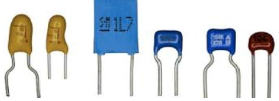
The Many Sizes & Shapes Of Capacitors
You'll find one or more capacitors in almost every electronic circuit you build. And capacitors come in all sorts of shapes and sizes, influenced mostly by three things: the type of material used to create the plates, the type of material used for the dielectric, and the capacitance.
The most common types of capacitors are:
Ceramic disk: The plates are made by coating both sides of a small ceramic or porcelain disk with silver solder. The ceramic or porcelain disk is the dielectric, and the silver solder forms the plates. Leads are soldered to the plates, and the entire thing is dipped in resin.
Ceramic disk capacitors are small and usually have low capacitance values, ranging from 1 pF to a few microfarads. Because they're small, their values are usually printed using a three-digit shorthand notation.
Ceramic disk capacitors aren't polarized, so you don't have to worry about polarity when you use them.
Silver mica: The dielectric is made from mica, and this capacitor is sometimes referred to simply as a mica capacitor. As with ceramic capacitors, the plates in a silver mica capacitor are made from silver. Electrodes are joined to the plates, and then the capacitor is dipped in epoxy.
Silver mica capacitors come in about the same capacitance range as ceramic disk capacitors. However, they can be made to much higher tolerances — as close as 1% in some cases. Like ceramic disk capacitors, silver mica capacitors aren't polarized.
Although ceramic disk and mica capacitors are constructed in a similar way, they're easy to tell apart. Ceramic disk capacitors are thin, flat disks and are nearly always a dull, light-brown color. Silver mica capacitors are thicker, bulge at the ends where the leads are attached, and are shiny and sometimes colorful — red, blue, yellow, and green are common colors for silver mica capacitors.
Film: The dielectric is made from a thin film-like sheet of insulating material, and the plates are made from film-like sheets of metal foil. In some cases, the plates and the dielectric are then tightly rolled together and enclosed in a metal or plastic can. In other cases, the layers are stacked and then dipped in epoxy.
Depending on the materials used, capacitance for film capacitors can be as small as 1,000 pF or as large as 100 μF. Film capacitors aren't polarized.
Electrolytic: One of the plates is made by coating a foil film with a highly conductive, semiliquid solution called electrolyte. The other plate is another foil film on which an extremely thin layer of oxide has been deposited; this thin layer serves as the dielectric. The two layers are then rolled up and enclosed in a metal can.
Electrolytic capacitors are polarized, so you must be sure to connect voltage to it in the proper direction. If you apply voltage in the wrong direction, the capacitor may be damaged and might even explode.
You find these two common types of electrolytic capacitors:
Aluminum: Can be quite large, with as much as a tenth of a farad or more (100,000 μF).
Tantalum: Are smaller, ranging up to about 1,000 μF.
Variable: A capacitor whose capacitance can be adjusted by turning a knob. One common use for a variable capacitor is to tune a radio circuit to a specific frequency.
In the most common type of variable capacitor, air is used as the dielectric, and the plates are made of rigid metal. Several pairs of plates are typically used in an intermeshed arrangement. One set of plates is fixed (not moveable), but the other set is attached to a rotating knob.
When you turn the knob, you change the amount of surface area on the plates that overlap. This, in turn, changes the capacitance of the device.

-
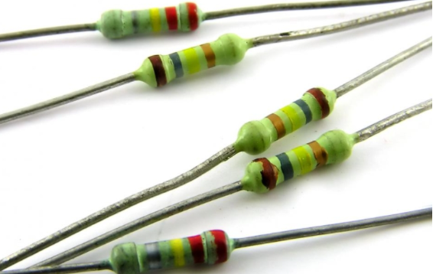
The resistor is the most common and well-known of the passive electrical components. A resistor resists or limits the flow of electric current in a circuit. There are many uses for resistors: they are used to drop voltage, limit current, attenuate signals, act as heaters, act as fuses, furnish electrical loads and divide voltages.
What is Ohm's Law?
Ohm’s law is a simple equation that shows the relationship between resistance, voltage and current through a metal wire, or some other type of resistive material. In mathematical terms, Ohm’s law is written as:
I = V/R
where I is the current (amps), V is the voltage, and R is the resistance.
Ohm’s law can also show the relationship between resistance, voltage and power using the following equation:
P = (V*V)/R
where P is the power (watts), V is the voltage, and R is the resistance.
Types of Resistors
Fixed Resistors
A fixed resistor is one in which the value of its resistance cannot change.
Variable Resistors
A variable resistor is a resistor whose value can be adjusted by turning a shaft or sliding a control. They are also called potentiometers or rheostats and allow the resistance of the device to be altered by hand.
Non-Linear Resistors
A non-linear resistor is a resistor that has resistances that vary significantly with applied voltage, temperature or light. Types of non-linear resistors are varistors, thermistors and photoresistors.
Common Resistor Terminology
Critical Resistance Value
The maximum nominal resistance value at which the rated power can be loaded without exceeding the maximum working voltage. The rated voltage is equal to the maximum working voltage in the critical resistance value.
De-rating Curve
The curve that expresses the relation between the ambient temperature and the maximum value of continuously loadable power at its temperature, which is generally expressed as a percentage.
Dielectric Withstanding Voltage
The rated voltage that can be applied to a designated point between the resistive element and the outer coating, or the resistive element and the mounting surface, without causing dielectric breakdown.
Electrostatic Discharge (ESD) Sensitivity
In resistors, ESD sensitivity is a function of their size. The smaller the resistor, the less space there is to spread the energy pulsed through it from the ESD. This energy concentration in a small area of a resistor’s active element causes it to heat up, which could lead to irreversible damage. With the growing trend of miniaturization, electronic devices, including resistors, are becoming smaller and smaller, causing them to be more prone to ESD damage.
Load Life Stability
Load life stability is the characteristic most relied upon to demonstrate a resistor’s long-term reliability. Military testing requirements to 10,000 hours with limits on amount of shift and the resistors value and the number of failures results in a failure rate evaluation. (Please see the "Precision Current Sensing" under our "applications" section on this website for a complete explanation.
Maximum Overload Voltage
The maximum value of voltage capable of being applied to resistors for a short period of time in the overload test. Typically the applied voltage in the short time overload test is 2.5 times larger than the rated voltage. However, it should not exceed the maximum overload voltage.
Maximum Working Voltage (or Maximum Limiting Element Voltage)
The maximum value of DC voltage or AC voltage (rms) capable of being applied continuously to resistors or element. However, the maximum value of the applicable voltage is the rated voltage at the critical resistance value or lower.
Noise
Noise is an unwanted AC signal from within the resistor. Resistive noise can have a devastating effect on low-level signals, charge amplifiers, high gain amplifiers, and other applications sensitive to noise. The best approach is to use resistor types with low or minimal noise in applications that are sensitive to noise.
Power Rating
Power ratings are based on physical size, allowable change in resistance over life, thermal conductivity of materials, insulating and resistive materials, and ambient operating conditions. For best results, employ the largest physical size resistors at less than their maximum rated temperature and power.
Rated Ambient Temperature
The maximum ambient temperature at which resistors are capable of being used continuously with the prescribed rated power. The rated ambient temperature refers to the temperature around the resistors inside the equipment, not to the air temperature outside the equipment.
Rated Power
The maximum amount of power that can be continuously loaded to a resistor at a rated ambient temperature. Network and array products have both rated power per package as well as per element.
Rated Voltage
The maximum value of DC voltage or AC voltage (rms) capable of being applied continuously to resistors at the rated ambient temperature.
Reliability
Reliability is the probability that a resistor (or any other device) will perform its desired function. There are two ways of defining reliability. One is Mean Time Between Failures (MTBF) and the other is Failure Rate per 1000 hours of operation. Both of these means of evaluating reliability must be determined with a specific group of tests and a definition of what is the end of life for a device, such as a maximum change in resistance or a catastrophic failure (short or open). Various statistical studies are used to arrive at these failure rates and large samples are tested at the maximum rated temperature with rated load for up to 10 000 hours (24 hours per day for approximately 13 months). Reliability is generally higher at lower power levels.
High Speed and Response Time
The equivalent circuit of a resistor, as shown in Figure 1, combines a resistor in series with an inductance and in parallel with a capacitance (PLC). Resistors can perform like an R/C circuit, filter or inductor depending on their geometry. In spiraled and wire-wound resistors, these reactances are created by the loops and spaces formed by the spirals or turns of wire.
Resistor Tolerance
Resistor tolerance is expressed as the deviations from nominal value in percent and is typically measured at 25 °C. A resistor’s value will also change with applied voltage (VCR) and temperature (TCR). For networks, absolute resistor tolerance refers to the overall tolerance of the network. Ratio tolerance refers to the relationship of each resistor to the others in the package.
Stability
Stability is the change in resistance with time at a specific load, humidity level, stress, or ambient temperature. When these stresses are minimized, the better the stability. Temperature Coefficient of Resistance (TCR also known as RTC) TCR is expressed as the change in resistance in ppm (0.0001 %) with each degree Celsius of change in temperature. TCR is typically referenced at + 25 ˚C and changes as the temperature increases (or decreases). A resistor with a TCR of 100 ppm/°C will change 0.1 % over a 10 °C change and 1 % over a 100 °C change. In the context of a resistor network, the TCR value is called the absolute TCR in that it defines the TCR of a specific resistor element. The term TCR tracking refers to the difference in TCR between each specific resistor in a network.
Temperature Rating
Temperature rating is the maximum allowable temperature at which the resistor may be used. It is generally defined with two temperatures. For example, a resistor may be rated at full load up to + 70 °C derated to no load at + 125 °C. This means that with certain allowable changes in resistance over the life of the resistor, it may be operated at + 70 °C at rated power. It also may be operated with temperatures in excess of + 70 °C if the load is reduced, but in no case should the temperature exceed the design temperature of + 125 ˚C with a combination of ambient temperature and self-heating due to the applied load.
Voltage Coefficient of Resistance (VCR)
The voltage coefficient is the change in resistance with applied voltage. This is entirely different and in addition to the effects of self-heating when power is applied. A resistor with a VCR of 100 ppm/V will change 0.1 % over a 10 V change and 1 % over a 100 V change. In the context of a resistor network, this VCR value is called the absolute VCR in that it defines the VCR of a specific resistor element. The term VCR tracking refers to the difference in VCR between each specific resistor in a network.
-
Diodes
– A diode is a tow-terminal electric component with asymmetric conductance; it has low (ideally zero) resistance to current in one direction, and high (ideally infinite) resistance in the other.
LED
– A light-emitting diode (LED) is a two-lead semiconductor light source. It is a basic pn-junction diode, which emits light when activated.[7] When a fitting voltage is applied to the leads, electrons are able to recombine with electron holes within the device, releasing energy in the form of photons. This effect is called electroluminescence, and the color of the light (corresponding to the energy of the photon) is determined by the energy band gap of the semiconductor.
PhotoDiode
– A photodiode is a semiconductor device that converts light into current. The current is generated when photons are absorbed in the photodiode. A small amount of current is also produced when no light is present. Photodiodes may contain optical filters, built-in lenses, and may have large or small surface areas. Photodiodes usually have a slower response time as its surface area increases. The common, traditional solar cell used to generate electric solar power is a large area photodiode.
Schottky Diode
– The Schottky diode (named after German physicist Walter H. Schottky); also known as hot carrier diode is a semiconductor diode with a low forward voltage drop and a very fast switching action. The cat’s-whisker detectors used in the early days of wireless and metal rectifiers used in early power applications can be considered primitive Schottky diodes.
TVS
– A transient-voltage-suppression (TVS) diode is an electronic component used to protect sensitive electronics from voltage spikes induced on connected wires.
Tunnel Diode
– A tunnel diode or Esaki diode is a type of semiconductor that is capable of very fast operation, well into the microwave frequency region, made possible by the use of the quantum mechanical effect called tunneling.
Varicap
– A varicap diode, varactor diode, variable capacitance diode, variable reactance diode or tuning diode is a type of diode whose capacitance varies as a function of the voltage applied across its terminals.
Zener Diode
– A Zener diode is a diode which allows current to flow in the forward direction in the same manner as an ideal diode, but also permits it to flow in the reverse direction when the voltage is above a certain value known as the breakdown voltage, “Zener knee voltage”, “Zener voltage”, “avalanche point”, or “peak inverse voltage.
-
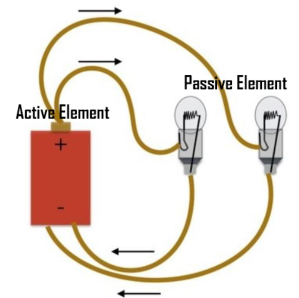
The Two Types of Electronic Devices
Electronic elements that make up a circuit are connected together by conductors to form a complete circuit.
Active components
Passive components
Active Components
An active component is an electronic component which supplies energy to a circuit.
Common examples of active components include:
Voltage sources
Current sources
Generators (such as alternators and DC generators)
All different types of transistors (such as bipolar junction transistors, MOSFETS, FETs, and JFET)
Diodes (such as Zener diodes, photodiodes, Schottky diodes, and LEDs)
Voltage Sources
A voltage source is an example of an active component in a circuit. When current leaves from the positive terminal of the voltage source, energy is being supplied to the circuit. As per the definition of an active element, a battery can also be considered as an active element, as it continuously delivers energy to the circuit during discharging.
Current Sources
A current source is also considered an active component. The current supplied to the circuit by an ideal current source is independent of circuit voltage. As a current source is controlling the flow of charge in a circuit, it is classified as an active element.
Transistors
Although not as obvious as a current or voltage source – transistors are also an active circuit component. This is because transistors are able to amplify the power of a signal (see our article on transisors as an amplifier if you want to know exactly how).
Passive Components
A passive component is an electronic component which can only receive energy, which it can either dissipate, absorb or store it in an electric field or a magnetic field. Passive elements do not need any form of electrical power to operate.
As the name ‘passive’ suggests – passive devices do not provide gain or amplification. Passive components cannot amplify, oscillate, or generate an electrical signal.
Common examples of passive components include:
Resistors
Inductors
Capacitors
Transformers
Resistors
A resistor is taken as a passive element since it can not deliver any energy to a circuit. Instead resistors can only receive energy which they can dissipate as heat as long as current flows through it.
Inductors
An inductor is also considered as passive element of circuit, because it can store energy in it as a magnetic field, and can deliver that energy to the circuit, but not in continuous basis. The energy absorbing and delivering capacity of an inductor is limited and transient in nature. That is why an inductor is taken as a passive element of a circuit.
Capacitors
A capacitor is considered as a passive element because it can store energy in it as electricfield. The energy dealing capacity of a capacitor is limited and transient – it is not actually supplying energy, it is storing it for later use.
As such it is not considered an active component since no energy is being supplied or amplified.
Transformers
A transformer is also a passive electronic component. Although this can seem surprising since transformers are often used to raise voltage levels – remember that power is kept constant.
When transformers step up (or step down) voltage, power and energy remain the same on the primary and secondary side. As energy is not actually being amplified – a transformer is classified as a passive element.
ACTIVE ELECTRONIC COMPONENTS
SEMICONDUCTORS
Diodes (All)
Light-Emitting Diode (LED)
Rectifier Diode
Schottky Diode
Solar PV Cell, PV Panel
Unipolar / Bipolar Diode
Varicap
Varactor
Zener Diode
TRANSISTORS
Composit Transistors
Compound Transistor
Darlington Transistor
Field-Effect Transistor (FET)
JFET (Junction Field-Effect Transistor)
MOSFET (Metal Oxide Semiconductor FET)
Photo Transistor
Transistors (All)
Thyristors
BASIC COMPONENTS
Antennas
Assembly Modules
Capacitors (All Types)
Detectors
Inductors / Coil
Memristor / Network
Resistors (All Types)
Sensors
Transducers
ELECTROMECHANICAL COMPONENTS
Cables
Circuit Protection Devices
Crystals
Mechanical Devices such as a Fan, Lamp
PCB
Piezoelectric devices
Resonators
Switches
Terminals and Connectors
WHAT’S THE DIFFERENCE?
Active Components
Active Device transforms and injects power or energy into a circuit.
Examples: Diode, Transistor, SCR, ICs, DC generator, Current & Voltage sources etc.
Active element produces energy in the form of voltage or current
They have function and provide power gain (Amplifier).
t can control the flow of current.
Active components require an external & conditional source to operate in the circuit.
They have gain more than 1, so they can amplify the signal.
They are energy donor.
They lay in Linear category
Passive Components
Passive Device utilizes power or energy into a circuit.
Examples: Resistors, Capacitors, Inductors, Transformer, Motors etc.
Passive element stores energy in the form of voltage or current.
They do not have function provide power gain.
It cannot control the flow of the current.
Passive Components do not require any external source to operate in the circuit.
They have gain less than 1, so they can’t amplify the signal.
They are energy acceptor
They lay in Non-Linear category.

-
In 2017 ES Components purchased all Military JFET/MOSFET and Analog Switch Inventories, Finished Goods, Assembly and Test Equipment from SILICONIX.
ES Components subcontracted our JAN JFET and MOSFETS (MIL 19500) Production and Test to VPT Components. Per the DLA the assemblies must be marked with the VPT brand not Siliconix or ES Components but, the internal Qualified SILICONIX Silicon chips made in Santa Clara and outperform the competition as they always have.
The Analog Switch and other Military components previously offered by SILICONIX are now Assembled and Qualified by ES Components to (Mil 38535) and carry the ES Components Brand not Siliconix and like the JAN JFETS have SILICONIX Qualified Siliconix chips Inside. The same Siliconix Military products with a different brand.
In addition to Military Qualified products, ES Components received millions of SILICONIX Hi Reliability finished goods and wafers of both JFETS/MOSFETS and Analog Switches, for non Mil 19500 and Mil 38535 assemblies to be tested and marked with the ES Components Brand not the Siliconix. Like the Military products all Die are SILICONIX manufactured and meet the same performance and quality standards.
SILICONIX also offered Specials, Custom, Non-Standard Military grade and Hi Reliability assemblies. ES Components has the ability to supply those same assemblies using SILICONIX Die, screened to all requirements or any other custom configuration a customer may need.
In conclusion SILICONIX Military and Industrial equivalents are still alive and available from ES Components. Bring us your requirements, we have seamless solutions.

-
Michelle to supply verbiage/