


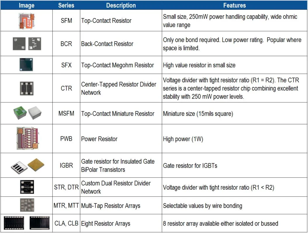
Wire Bondable Bare Die Resistors
Custom Designs With Unique Values, Sizes, and Configurations
In A Wide Range of Substrate Materials and Film Compositions That Provide
Maximum Flexibility and High-End Applications
Vishay EFI offers standard thin film wire bondable resistors to fit a wide variety of hybrid circuit applications. Standard products are fabricated on an oxidized silicon substrate using tantalum nitride as the resistor element and with aluminum contact pads. However, these resistors may be customized for other applications by using different materials. The resistors are also available on quartz, alumina, and AlN substrates; the resistor film can be nickel chromium; gold contact pads are also available, and gold backing can be provided.
Applications
High-reliability military, space, and medical components
Hybrid applications where epoxy die attach and wire bonding are the assembly technique
Lumped element filters
Impedance tuning networks
Analog designs requiring high precision and/or high levels of customization
Applications requiring miniature form factors
Wire-Bondable Bare Die Capacitors
Vishay EFI capacitors are based on Silicon Oxide (MOS) and Silicon Oxide / Nitride (MNOS) combinations. The high-quality dielectric film deposited by our state-of-the-art equipment is the key factor for the high performance that characterizes these capacitors.
A wide range of values and sizes helps simplify the integration of these products into new and existing applications. A wide range of values and sizes helps simplify the integration of these products into new and existing applications.
Features
NC Series sizes range from 20 x 20 mils to 60 x 60 mils
Tight value tolerances
Low TCC (Temperature Coefficient of Capacitance): (+ 45 ± 25 ppm/°C MNOS, + 15 ± 25 ppm°/C MOS)
Excellent life value stability
Wide range of values (0.5 pF to 1000 pF)
Vishay High Frequency Wire-Bondable Spiral Inductors
Spiral inductors are designed for RF circuits that require wire-bondable components. High precision equivalent circuit modeling enables accurate computer simulation of component performance. Additional values and form factors available upon request.
Applications
• RF choking for DC biasing
• RF tuning circuits
• Lumped element filters
Features
• High frequency
• Wire bond assembly
• Low DCR, high Q
• Low parasitic capacitance, high SRF
• Equivalent circuit model enclosed
• S parameter files available for download
• Sample kit available
Note: Additional values and form factors available upon request.
Substrates and Interconnects
Vishay Electro-Films offers very robust solid metal filled vias.
Call ES Components today to discuss your requirements in detail to jointly develop the optimum metalization structure for your application.
Features
Copper power lines up to 5000 microinches thick
Gold small signal lines ± 100 microinches width tolerance
Temperatures to 350 °C
Substrate material: Alumina, Beryllium Oxide or Aluminum Nitride
Excellent adhesion
Metallized through holes
Filled vias
Resistors available
Sizes up to 4 inches x 4 inches
Vishay is a leading-edge manufacturer of thin film custom substrates using alumina (Al2O3), aluminum nitride (AlN), beryllium oxide (BeO), quartz, silicon, ferrites, titanates and a wide range of metallization alternatives such as nichrome, tantalum nitride, titanium tungsten, copper, nickel, gold and aluminum.
Vishay Electro-Films
Vishay Electro-Films (EFI) has developed a thin film process that has the unique capability of incorporating up to 5000 microinches thick plated copper conductors on the same substrate with standard 100 to 300 microinches thick conductors. Some hybrid circuit applications require thick copper conductors for the power lines but standard thickness small signal lines to maintain tight line width control of critical elements. For example, a microwave application may require high power bias current to GaAs or other semiconductor devices while also requiring tight line width control to obtain good high frequency performance for lange couplers, filters or other critical signal patterns. For standard, high power, low frequency hybrid circuit substrates, thick copper plating alone is ideal. The 5000 microinches thick plated copper has a resistivity of less than 0.15 mΩ/square. In most cases, the dc or low frequency copper power lines are overplated with nickel and gold to prevent oxidation, permitting high temperature processing and operation. The conductor material for the small signal lines is normally gold. Several substrate materials and various adhesion metals are available.
Examples of Special Capabilities
OPTICAL SUB-MOUNTS
Custom ceramic circuit board based on highly thermally conductive materials such as AlN and BeO
This copper patterning capabilities up to 0.006” thick (150 um)
Solid filled vias
Gold/Tin solder deposition and patterning facilitating low thermal resistance die attach
SDWP – SIDE WALL PATTERNING
SDWP – capability for custom substrates
Replaces wirebonds
Side patterned connections have lower inductance and therefore operate better at high frequency
SDWP allows die assembly on the side wall of the ceramic chip. This allows better integration with the optical elements of the design (fibers, prisms, lenses etc.)
Allows up to 4 sides to be patterned: top, bottom and two additional opposite side walls
Available with Al2O3 or AlN substrates
Plate thickness <= 0.025” (planned to 0.040”)
Line width and gap >= 0.003”
Line and gap tolerances as low as +/- 0.001”
Metal pattern to dice edge tolerance down to +/-0.002”
TRANSMISSION LINE COMPONENTS
RF simulations during design review
Reflection coefficients (S11)
Insertion loss (S21)
Multiple variations for experimentation and process optimization